-
Magnetic SSRM SurfaceChange Stiffness Etch NCM Optic flakes Sidewall Wonseok Neodymium plastics F14H20 Conductive AFM BTO InorganicCompound HBN polymeric_arrays MESA structure Anneal Battery Polyaniline TappingMode India GalliumPhosphide membrane Temperature KAIST AM-KPFM Vinylpyridine Polyethylene ring shape Display Leakage polyvinyl acetate
Report image
If you found this image unacceptable, please let us know. We will review your report and take action if we determine this image is really unacceptable.
Atomic steps on GaP(Gallium Phosphide) layer on Si
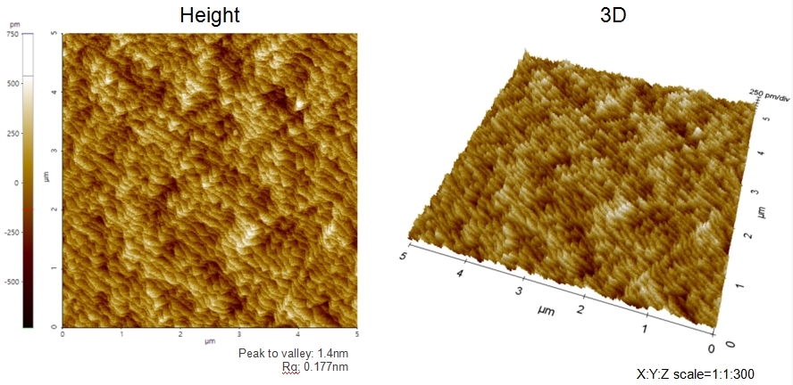
Scanning Conditions
- System: NX20
- Scan Mode: Non-contact
- Cantilever: PPP-NCHR (k=42N/m, f=300kHz)
- Scan Size: 5μm×5μm
- Scan Rate: 1Hz
- Pixel: 512×512