-
Chemical Vapor Deposition Spain conductive Hexylthiophene silicon_oxide Domain IndiumTinOxide TungstenDeposition PetruPoni Conductance CVD PANI LiftMode self-assembly MechanicalProperties CP-AFM UTEM Tape PolyimideFilm Titanate SingleCrystal HBN FM_KPFM LFM TungstenThinFilmDeposition alkanes gallium_nitride Polyethylene Graphite DomainSwitching Liquid ScanningTunnelingMicroscopy Tapping hard_disk KAIST
Report image
If you found this image unacceptable, please let us know. We will review your report and take action if we determine this image is really unacceptable.
Taegeuk Mark Lithography on PZT
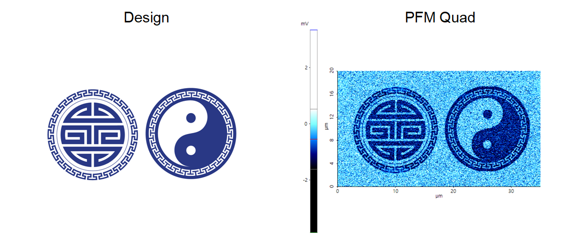
Re-arranged the domain pole direction on PZT surface using bias mode of lithography.
Scanning Conditions
- System: NX10
- Scan Mode: Lithography
- Cantilever: PPP-ContScPt (k=0.2N/m, f=25kHz)
- Scan Size: 35μm×20μm
- Scan Rate: 0.5Hz
- Pixel Size: 1024 × 1024
- Tip Bias: 10V for patterned area
- Scan Mode: Lithography
- Cantilever: PPP-ContScPt (k=0.2N/m, f=25kHz)
- Scan Size: 35μm×20μm
- Scan Rate: 0.5Hz
- Pixel Size: 1024 × 1024
- Tip Bias: 10V for patterned area