-
Electrical&Electronics GaP Chemical_Vapor_Deposition temperature_control HardDiskMedia conductive #Materials NUS Anneal GlassTemperature Ptfe Domain FailureAnlaysis cannabinoid Nanofiber CrystalGrowing MfmAmplitude MagneticArray Jason LithiumNiobate Christmas Mfm Tin disulfide Multiferroic_materials ThermalDetectors Transparent molecule light_emission Biofilm Wang DiffractiveOpticalElements Lift Pzt BiFeO3 PolyvinylideneFluoride
Report image
If you found this image unacceptable, please let us know. We will review your report and take action if we determine this image is really unacceptable.
ITO Film Sputter Deposited onto Silicon
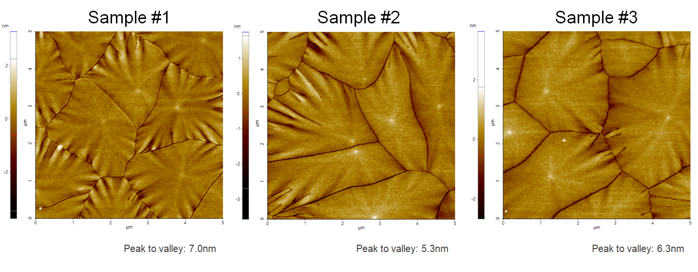
ITO-film, which was sputter deposited onto silicon. The grain size of those samples was influenced by changing the process settings in the Cluterline RAD sputter deposition system, one of the deposition tool platforms manufactured by Evatec.
Scanning Conditions
- System: NX10
- Scan Mode: Non-contact
- Cantilever: PPP-EFM (k=2.8N/m, f=75kHz)
- Scan Size: 5μm×5μm
- Scan Rate: 0.1Hz
- Pixel Size: 256 × 256
- Scan Mode: Non-contact
- Cantilever: PPP-EFM (k=2.8N/m, f=75kHz)
- Scan Size: 5μm×5μm
- Scan Rate: 0.1Hz
- Pixel Size: 256 × 256