-
Annealing Regensburg PatternedSapphireSubstrat MetalCompound Styrene DomainSwitching Leakage Gallium_Arsenide Gallium Dopped Conductance Collagen Hexylthiophene Fluoride ElectrostaticForceMicroscopy Mechinical TungstenDeposition IRDetector PMNPT Alloy India graphene_hybrid Writing AM_KPFM Film Gong KPFM pulsed_laser_deposition Co/Cr/Pt Holes #Materials temperature controller AFM Alkane Wafer Display
Report image
If you found this image unacceptable, please let us know. We will review your report and take action if we determine this image is really unacceptable.
Carbon Nanotube on Si
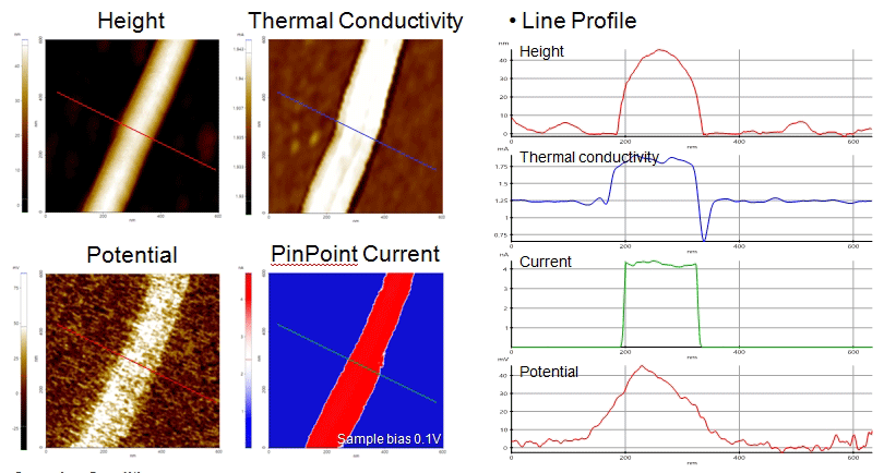
Scanning Conditions
- System: XE7
- Scan Mode: SThM, KPFM, PinPoint CP-AFM
- Cantilever: Nanothermal probe, NCST-Au (k=7.4N/m, f=160kHz), CDT-CONTR (k=0.5N/m, f=20kHz)
- Scan Size: 0.6μm×0.6μm
- Scan Rate: 0.5Hz, 0.5Hz, 0.15Hz
- Pixel: 256×128
- Scan Mode: SThM, KPFM, PinPoint CP-AFM
- Cantilever: Nanothermal probe, NCST-Au (k=7.4N/m, f=160kHz), CDT-CONTR (k=0.5N/m, f=20kHz)
- Scan Size: 0.6μm×0.6μm
- Scan Rate: 0.5Hz, 0.5Hz, 0.15Hz
- Pixel: 256×128