-
Blend VortexCore Lanthanum_aluminate Liquid heterojunctions WPlug SICM Polydimethylsiloxane Christmas ThermalProperties Heating Fujian HanyangUniv IcelandSpar mono_layer strontiu_titanate CrAu LiquidImaging BloodCell HardDisk Magnetostrictive DomainSwitching Vac Self-assembledMonolayer Transparent ContactMode Hafnium_dioxide Topography MagneticPhase DeflectionOptics HBN Polytetrafluoroethylene 2d_materials tip_bias_mode NCM\
Report image
If you found this image unacceptable, please let us know. We will review your report and take action if we determine this image is really unacceptable.
Multi-layer necking device defect
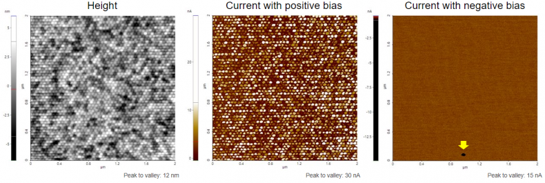
Scanning Conditions
- System : NX-Wafer
- Scan Mode: C-AFM
- Scan Rate : 2Hz
- Scan Size : 2μm×2μm
- Pixel Size : 512×256
- Cantilever : AD-2.8-AS (k=2.8N/m, f=75kHz)