-
semifluorinated_alkanes MolybdenumDisulfide Gallium SiliconeOxide Chrome BiFeO3 Solution Tin sulfide FailureAnlaysis self-assembled_monolayer Film light_emission Hafnia Aggregated_molecules CNT Layer ThermalDetectors Ferroelectric dielectric_trench Adhesive biocompatible thermal_property SSRM Semiconductor ContactMode light_emitting TipBiasMode OrganicCompound LiNbO3 TungstenDeposition CalciumHydroxide Phenanthrene Butterfly ThermalProperties IndiumTinOxide
Report image
If you found this image unacceptable, please let us know. We will review your report and take action if we determine this image is really unacceptable.
Moire pattern of MoS₂-WSe₂
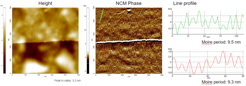
Scanning Conditions
- System : FX40
- Scan Mode: Tapping
- Scan Rate : 3Hz
- Scan Size : 500nm×500nm
- Pixel Size : 512×512
- Cantilever : PPP-FMR (k=2.8N/m, f=75kHz)