-
Materials TriGlycineSulphate LMF KPFM Aluminum India EPFL DomainSwitching Vac DIWafer IcelandSpar Anneal SingleLayer Cell GlassTemperature Wildtype EFM Gallium Heat Phosphide InLiquid ForceVolume GaAs optoelectronics mono_layer China Formamidinium_lead_iodide LowDensityPolyethylene HumanHair Sphere NUS_Physics MultiLayerCeramicCapacitor Aggregated_molecules TungstenThinFilmDeposition Hexatriacontane
Report image
If you found this image unacceptable, please let us know. We will review your report and take action if we determine this image is really unacceptable.
GaN epi wafer
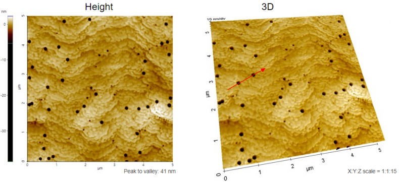
Scanning Conditions
- System : NX-Wafer
- Scan Mode: Non-contact
- Scan Rate : 0.7 Hz
- Scan Size : 5μm×5μm
- Pixel Size : 512×512
- Cantilever : PPP-NCHR (k=42N/m, f=330kHz)