-
NusEce Strontium PhthalocyaninePraseodymium pinpoint mode dichalcogenide NTU Edwin AIN Bismuth Growing Mosfet LogAmplifier GlassTemperature Layer silicon_oxide HiVacuum Subhajjit China HfO2 ItoGlass TPU Annealed Spincast Genetic AM-KPFM Sperm Tungsten OpticalWaveguides KevlarFiber Phenanthrene Step Force-distance Switching pulsed_laser_deposition margarine
Report image
If you found this image unacceptable, please let us know. We will review your report and take action if we determine this image is really unacceptable.
Trench Etch Profile on Si Wafer
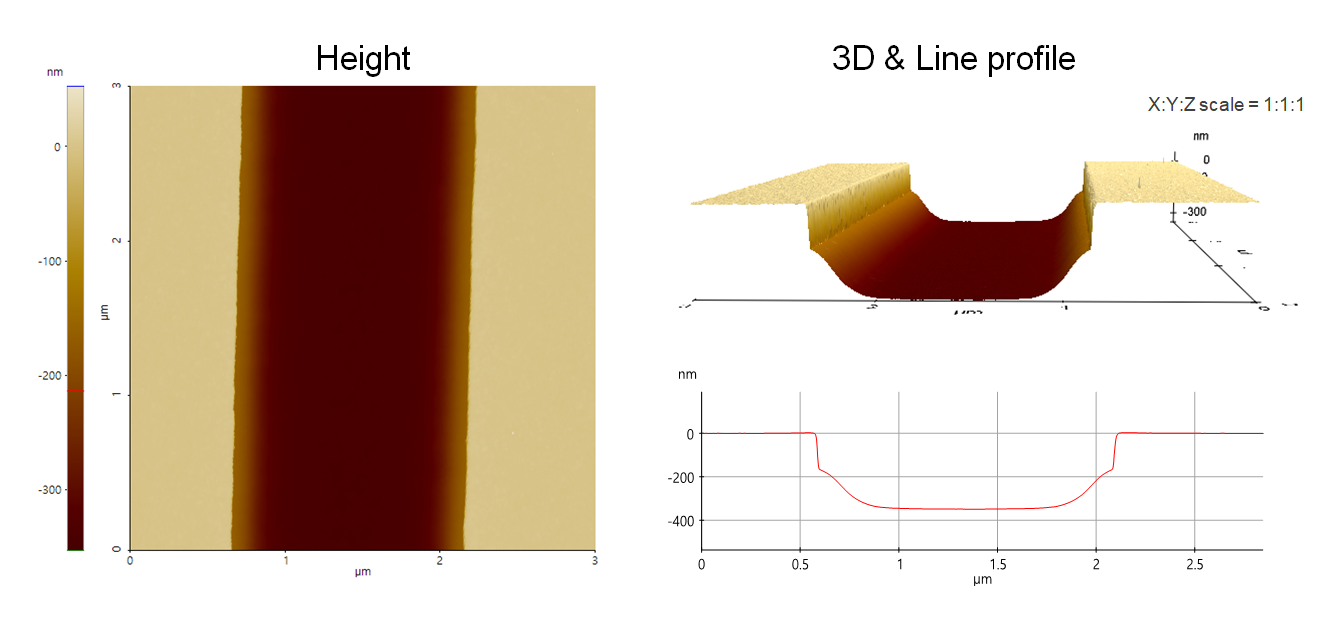
Top dielectric trench etch profile on Si wafer having tapered slope at the trench sidewall.
Scanning Conditions
- System: NX20
- Scan Mode: Non-contact
- Cantilever: AC160TS (k=26N/m, f=300kHz)
- Scan Size: 3μm×3μm
- Scan Rate: 0.21Hz
- Pixel: 1024 × 256
- Scan Mode: Non-contact
- Cantilever: AC160TS (k=26N/m, f=300kHz)
- Scan Size: 3μm×3μm
- Scan Rate: 0.21Hz
- Pixel: 1024 × 256