-
fluoroalkane CrAu Lanthanum_aluminate Lift HexagonalBN Polyurethane BlockCopolymer FM_SKPM NCM FrequencyModulation LiNbO3 Conductance Imprint YttriaStabilizedZirconia HighAspect Hysteresys BCZT IVSpectroscopy KelvinProbeForceMicroscopy Hafnium_dioxide light_emitting LightEmiting Korea GaAs polyvinyl acetate Platinum Calcite FastScan Ecoli PVA Hafnia VinylAlcohol Defects MeltingPoint silicon_oxide
Report image
If you found this image unacceptable, please let us know. We will review your report and take action if we determine this image is really unacceptable.
Atomic steps on GaP(Gallium Phosphide) layer on Si
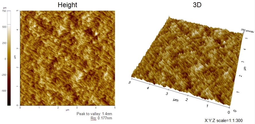
Scanning Conditions
- System: NX20
- Scan Mode: Non-contact
- Cantilever: PPP-NCHR (k=42N/m, f=300kHz)
- Scan Size: 5μm×5μm
- Scan Rate: 1Hz
- Pixel: 512×512