-
Lateral_Force_Microscopy DIWafer alkanes OrganicCompound SiliconeOxide Wafer 2-vinylpyridine Phthalocyanine VinylAlcohol IMT_Bucharest Gallium FFM DataStorage Optical Austenite Potential suspended_graphene DNAProtein IcelandSpar PS_LDPE Litho PinPointMode NUS_Physics Semiconductor Bacterium UnivCollegeLondon SAM Dental Tungsten_disulfide self-assembled_monolayer MagneticForce Ni81Fe19 Polyurethane Adhesive Growing
Report image
If you found this image unacceptable, please let us know. We will review your report and take action if we determine this image is really unacceptable.
Multi-layer necking device defect
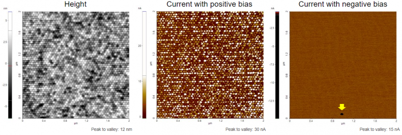
Scanning Conditions
- System : NX-Wafer
- Scan Mode: C-AFM
- Scan Rate : 2Hz
- Scan Size : 2μm×2μm
- Pixel Size : 512×256
- Cantilever : AD-2.8-AS (k=2.8N/m, f=75kHz)