-
flakes TemperatureControllerStage ContactModeDot MolecularSelfAssembly HardDiskMedia temp Temasek_Lab Piezoelectric PECurve FrictionalForceMicroscopy nanomechanical Anneal PhaseImaging Materials BiFeO3 food DeoxyribonucleicAcid HighAcpectRatio Glass Ceramics ThinFilm CuParticle thermal_conductivity Fluoride Reading silicon_carbide contact Monisha Friction MembraneFilter Edwin Piezo Microchannel FrequencyModulation Ecoli
Report image
If you found this image unacceptable, please let us know. We will review your report and take action if we determine this image is really unacceptable.
Taegeuk Mark Lithography on PZT
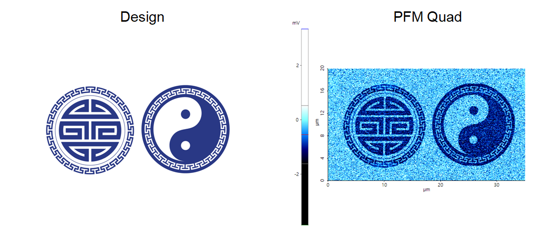
Re-arranged the domain pole direction on PZT surface using bias mode of lithography.
Scanning Conditions
- System: NX10
- Scan Mode: Lithography
- Cantilever: PPP-ContScPt (k=0.2N/m, f=25kHz)
- Scan Size: 35μm×20μm
- Scan Rate: 0.5Hz
- Pixel Size: 1024 × 1024
- Tip Bias: 10V for patterned area
- Scan Mode: Lithography
- Cantilever: PPP-ContScPt (k=0.2N/m, f=25kHz)
- Scan Size: 35μm×20μm
- Scan Rate: 0.5Hz
- Pixel Size: 1024 × 1024
- Tip Bias: 10V for patterned area