-
Litho Co/Cr/Pt dichalcogenide Mechanical TungstenDeposition phase_change mechanical property Mechinical Photovoltaics LifeScience Trench Gong Adhesion fluoroalkane Austenite single_layer multi_layer alkanes graphene_hybrid silicon_carbide Writing Liquid Epoxy NeodymiumMagnets Phthalocyanine doped UnivOfMaryland WWafer GlassTemp Solution Optical Oxide Singapore AdhesionForce Copper
Report image
If you found this image unacceptable, please let us know. We will review your report and take action if we determine this image is really unacceptable.
ITO Film Sputter Deposited onto Silicon
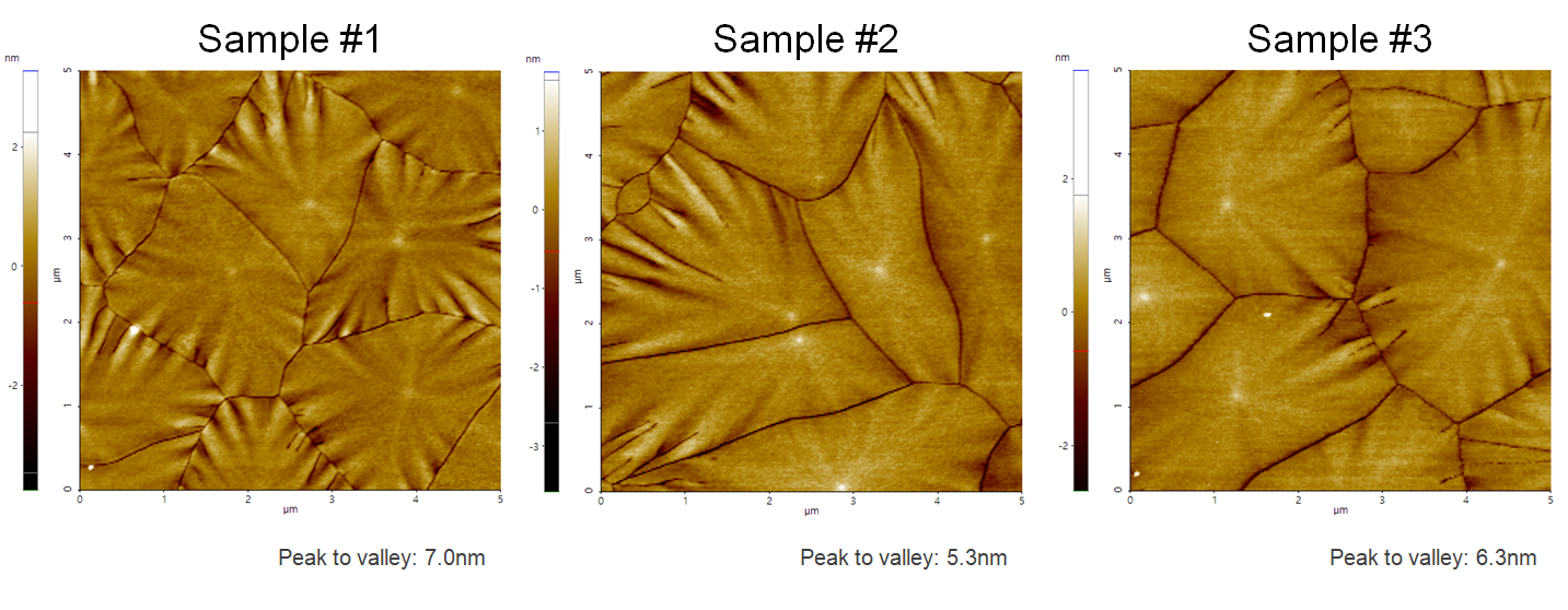
ITO-film, which was sputter deposited onto silicon. The grain size of those samples was influenced by changing the process settings in the Cluterline RAD sputter deposition system, one of the deposition tool platforms manufactured by Evatec.
Scanning Conditions
- System: NX10
- Scan Mode: Non-contact
- Cantilever: PPP-EFM (k=2.8N/m, f=75kHz)
- Scan Size: 5μm×5μm
- Scan Rate: 0.1Hz
- Pixel Size: 256 × 256
- Scan Mode: Non-contact
- Cantilever: PPP-EFM (k=2.8N/m, f=75kHz)
- Scan Size: 5μm×5μm
- Scan Rate: 0.1Hz
- Pixel Size: 256 × 256