-
Fendb Au111 Pvdf OrganicCompound SKKU atomic_steps Optoelectonics Non-ContactMode VortexCore DeoxyribonucleicAcid Silver HexagonalBN SrO Kevlar CeNSE_IISc Multiferroic_materials Magnets NUSNNI CastIron NanoLithography Dopped NiFe GranadaUniv dichalcogenide SelfAssembly cannabidiol OxideLayer Defect BFO Piezoresponse Sadowski ElectroChemical UnivMaryland Gold PvdfFilm
Report image
If you found this image unacceptable, please let us know. We will review your report and take action if we determine this image is really unacceptable.
Photoresist pattern (post-development process)
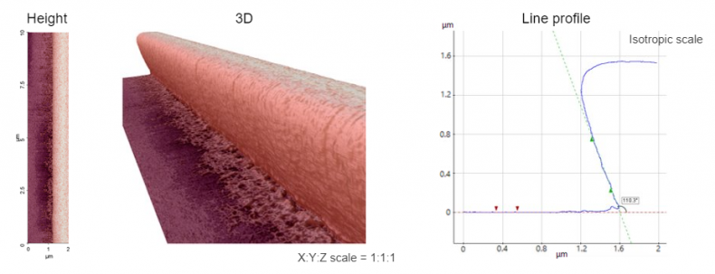
Scanning Conditions
- System : NX-3DM
- Scan Mode: Non-contact
- Scan Rate : 0.1 Hz
- Scan Size : 2μm×10μm
- Pixel Size : 512×2048
- Cantilever : EBD-R2-NCLR (k=45N/m, f=190kHz)