-
AIN ScratchMode LateralPFM dielectric trench SKKU Worcester_Polytechnic_Institute PVAC Wang Self-assembledMonolayer ferromagnetic plastic UTEM PS_LDPE HiVacuum Dopped PhaseImaging CarbonNanotube ContactMode Edwin LiBattery TemperatureControlledAFM ShenYang Pyroelectric NtuEee Mfm ContactModeDots HumanHair TCS ForceVolumeMapping TyphimuriumBiofilm cannabidiol Pinpoint non_contact Graphite LDPE
Report image
If you found this image unacceptable, please let us know. We will review your report and take action if we determine this image is really unacceptable.
Chip
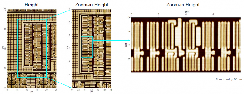
Scanning Conditions
- System : NX-Wafer
- Scan Mode: Non-contact
- Scan Rate : All 1Hz
- Scan Size : 25μm×40μm, 15μm×40μm, 8μm×4μm
- Pixel Size : 2048×256, 2048×256, 1024×256
- Cantilever : OMCL-AC160TS(k=26N/m, f=300kHz)