-
bias_mode thermal_conductivity STM Nanotechnology Optoelectonics PatternedSapphireSubstrat DomainSwitching Hexylthiophene Dental Optoelectronic KPFM CopperFoil biocompatible SurfaceOxidation frequency_modulation Polyvinylidene Hole Thermoplastic_polyurethane TyphimuriumBiofilm DNA C_AFM Treatment Metal BreastCancerCell Tin disulfide Spain IISCBangalore Hafnium_dioxide Worcester_Polytechnic_Institute F14H20 CuSubstrate TCS MagneticForce PolymerBlend Lateral_Force_Microscopy
Report image
If you found this image unacceptable, please let us know. We will review your report and take action if we determine this image is really unacceptable.
WLI image of wafer ID mark
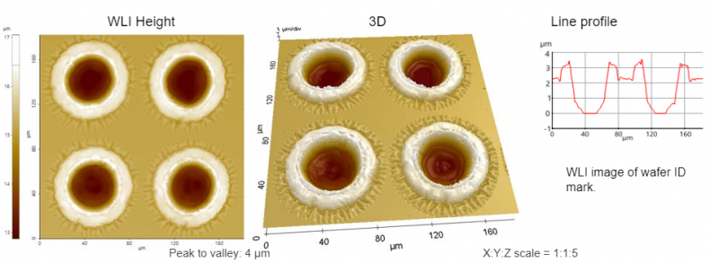
Scanning Conditions
- System : NX-Hybrid WLI
- Scan Mode: WLI
- Field of view: 182μm×182μm