-
Hafnium_dioxide GaN BiVO4 SiliconeOxide Pinpoint PFM ScanningIon-ConductanceMicroscopy Magnetic Force Microscopy AdhesionForce KelvinProbeForceMicroscopy Bismuth Roughness Magnetic Subhajjit Piezoresponse phase_change ChemicalCompound GlassTemperature Sio2 contact SurfaceChange PhaseTransition Yttria_stabilized_Zirconia H-BN Vacuum fluorocarbon dielectric trench PinPointMode FloppyDisk heterojunctions Singapore nanomechanical TemperatureControlledAFM Tungsten OrganicCompound OrganicSemiconductor
Report image
If you found this image unacceptable, please let us know. We will review your report and take action if we determine this image is really unacceptable.
CMP test key
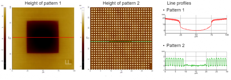
Scanning Conditions
- System : NX-Wafer
- Scan Mode: Non-contact
- Scan Rate : 1Hz for 100μm2 / 1.5Hz for 30μm2
- Scan Size : 100μm2, 30μm2
- Pixel Size : All 1024×512
- Cantilever : CMCL-AC240TS (k=2N/m, f=70kHz)