-
Molybdenum_disulfide conductive SurfaceChange DeflectionOptics Blend Optoelectonics MonoLayer Cobalt-dopedIronOxide NtuEee FailureAnalysis Mosfet self-assembly PinPointMode Ni-FeAlloy CP-AFM align graphene_hybrid OpticalWaveguide molecules sputter LateralForceMicroscopy Varistor ring shape cannabidiol AdhesionEnergy KevlarFiber Yeditepe_University HfO2 StrontiuTitanate Biology Organic Ucl IMT_Bucharest Self-assembledMonolayer Lanthanum_aluminate
Report image
If you found this image unacceptable, please let us know. We will review your report and take action if we determine this image is really unacceptable.
GaN on Si epi film
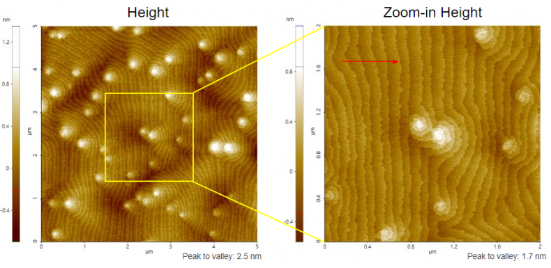
Scanning Conditions
- System : NX20
- Scan Mode: Non-contact
- Scan Rate : All 2 Hz
- Scan Size : 5µm2, 5µm2
- Pixel Size : ALL 512×512
- Cantilever : OMCL-AC160TS (k=26N/m, f=300kHz)