-
Yttria_stabilized_Zirconia nanobar ElectroDeposition molecule Piezoresponse China CNT Mechanical Conductance Copper Spincast cannabinoid ConductiveAFM hard_disk_media AmplitudeModulation Cobalt epitaxy Roughness PVA contact neodymium_magnets Wang PolymerPatterns semifluorinated_alkanes F14H20 Annealed ScanningIon-ConductanceMicroscopy PetruPoni_Institute Fe_film Neodymium Pores Etch SThM Mobile TipBiasMode
Report image
If you found this image unacceptable, please let us know. We will review your report and take action if we determine this image is really unacceptable.
Monolayer Graphene on PDMS Surface
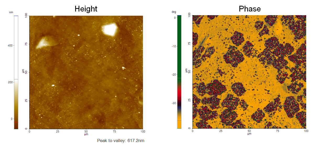
Monolayer Graphene grown on Cu foil using CVD process is transferred on to PDMS substrate.
Scanning Conditions
- System: NX20
- Scan Mode: Tapping
- Cantilever: Access-NC (k=113N/m, f=330kHz)
- Scan Size: 100μm×100μm
- Scan Rate: 0.6Hz
- Pixel Size: 256 × 256
- Scan Mode: Tapping
- Cantilever: Access-NC (k=113N/m, f=330kHz)
- Scan Size: 100μm×100μm
- Scan Rate: 0.6Hz
- Pixel Size: 256 × 256