-
CompactDisk Switching Metal-organicComplex IcelandSpar Ni-FeAlloy Treatment PECurve EFMAmplitude CarbonNanotube Polystyrene Croatia Gong Annealing Mapping Fet ThermalProperties Non-ContactMode MLCC Terrace Piezoelectric Spain ConductiveAFM Magnets Dr.JurekSadowski Wang LMF Fiber Potential Sadowski CuSubstrate ContactMode UTEM thermoplastic_elastomers HanyangUniv Memory
Report image
If you found this image unacceptable, please let us know. We will review your report and take action if we determine this image is really unacceptable.
Taegeuk Mark Lithography on PZT
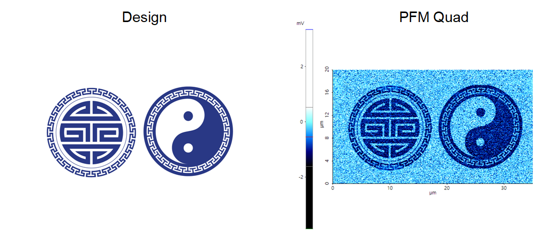
Re-arranged the domain pole direction on PZT surface using bias mode of lithography.
Scanning Conditions
- System: NX10
- Scan Mode: Lithography
- Cantilever: PPP-ContScPt (k=0.2N/m, f=25kHz)
- Scan Size: 35μm×20μm
- Scan Rate: 0.5Hz
- Pixel Size: 1024 × 1024
- Tip Bias: 10V for patterned area
- Scan Mode: Lithography
- Cantilever: PPP-ContScPt (k=0.2N/m, f=25kHz)
- Scan Size: 35μm×20μm
- Scan Rate: 0.5Hz
- Pixel Size: 1024 × 1024
- Tip Bias: 10V for patterned area