-
atomic_layer PinpointNanomechanicalMode thermal_property RedBloodCell HexacontaneFilm Magnets ChemicalCompound Aluminium_Oxide Polyvinylidene Chloroform ForceVolumeMapping ElectroDeposition Transparent domain_switching Bismuth CHRYSALIS_INC Device Dental IcelandSpar PetruPoni NiFe AlkaneFilm Patterns NUS AtomicLayer Sapphire Alkane atomic_steps TemperatureControl Cancer Hair Current Ferroelectric Carbon chemical_compound
Report image
If you found this image unacceptable, please let us know. We will review your report and take action if we determine this image is really unacceptable.
MoS2 Layers on SiO2
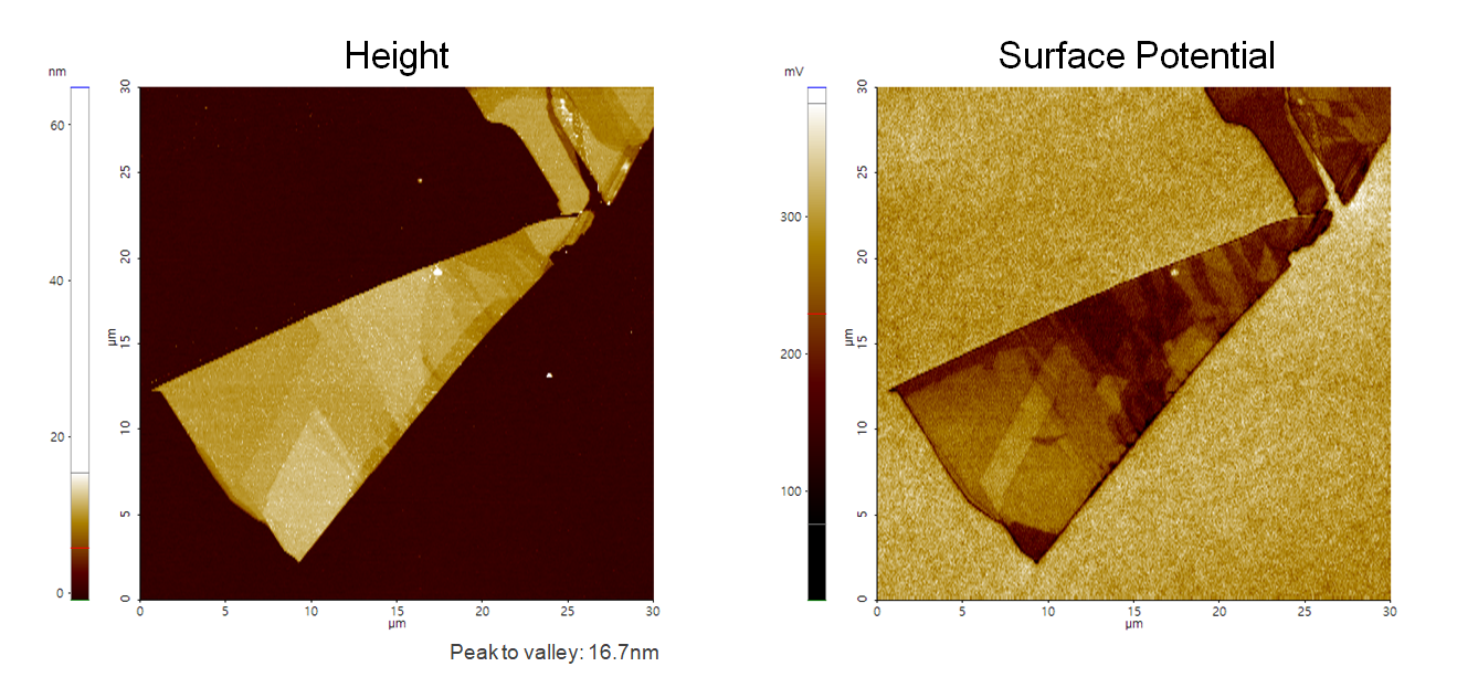
A few layers of MoS2 on SiO2
Scanning Conditions
- System: NX10
- Scan Mode: AM-KPFM
- Cantilever: NSC36Cr-Au B (k=2N/m, f=130kHz)
- Scan Size: 30μm×30μm
- Scan Rate: 0.3Hz
- Pixel Size: 512 × 256
- Scan Mode: AM-KPFM
- Cantilever: NSC36Cr-Au B (k=2N/m, f=130kHz)
- Scan Size: 30μm×30μm
- Scan Rate: 0.3Hz
- Pixel Size: 512 × 256