-
thermal_conductivity University_of_Regensburg dichalcogenide Floppy Cell DomainSwitching Boundary PolycrystallineFerroelectricBCZT MagneticPhase Pores CopperFoil CBD temperature_control DNAProtein kelvin probe force microscopy Bio Growth AM_KPFM atomic_layer MBE Indium_tin_oxide Grain Blood Sperm INSP Co/Cr/Pt Permalloy Hafnium_dioxide UnivOfMaryland ScanningThermalMicroscopy 2dMaterials AnodizedAluminumOxide Filter NTU Barium_titanate
Report image
If you found this image unacceptable, please let us know. We will review your report and take action if we determine this image is really unacceptable.
Trench Etch Profile on Si Wafer
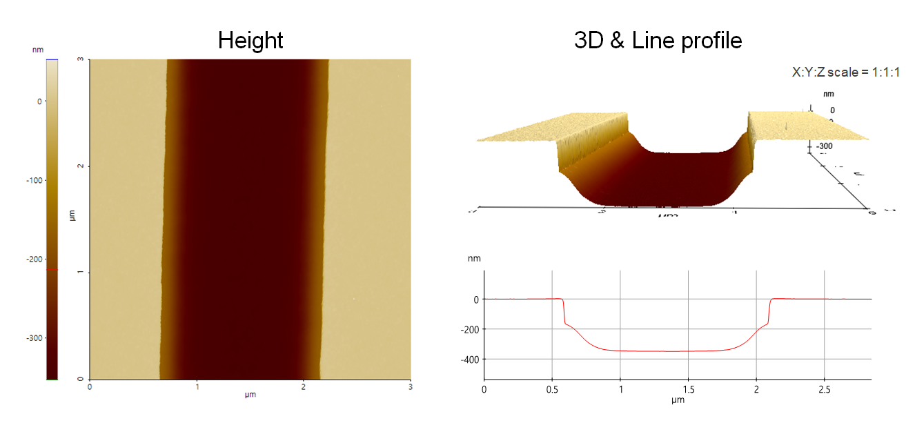
Top dielectric trench etch profile on Si wafer having tapered slope at the trench sidewall.
Scanning Conditions
- System: NX20
- Scan Mode: Non-contact
- Cantilever: AC160TS (k=26N/m, f=300kHz)
- Scan Size: 3μm×3μm
- Scan Rate: 0.21Hz
- Pixel: 1024 × 256
- Scan Mode: Non-contact
- Cantilever: AC160TS (k=26N/m, f=300kHz)
- Scan Size: 3μm×3μm
- Scan Rate: 0.21Hz
- Pixel: 1024 × 256