-
DeflectionOptics SiliconOxide Topography HydroGel PatternedSapphireSubstrat Tungsten thermal_property FuelCell PolyimideFilm cannabidiol lift_mode nanomechanical Collagen HardDiskMedia OrganicSemiconductor AtomicLayer PpLdpe molecular_beam ForceVolume Korea atomic_steps ConductingPolymer Ptfe SRAM semifluorinated_alkanes Copper EvatecAG Leakage ElectroDeposition amplitude_modulation Writing Indent Adhesive Terrace HexagonalBoronNitride
Report image
If you found this image unacceptable, please let us know. We will review your report and take action if we determine this image is really unacceptable.
Polymer patterns on Si (1/2)
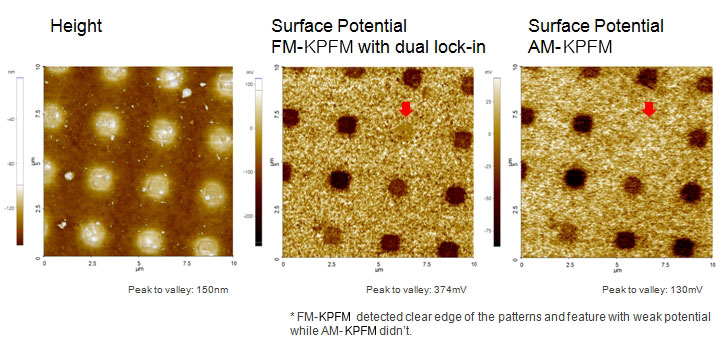
Scanning Conditions
- System: NX10
- Scan Mode: KPFM
- Cantilever: NSC36Cr-Au (k=1N/m, f=90kHz)
- Scan Size: 10μm×10μm
- Scan Rate: 0.2Hz
- Pixel: 512×256