-
Hafnium_dioxide atomic_steps TriGlycineSulphate Electrical&Electronics Growth MetalCompound Hexatriacontane FrequencyModulation SKPM Iron MultiLayerCeramicCapacitor Dr.JurekSadowski Sio2 OxideLayer ThermalDetectors Polyvinylidene WWafer Cross-section EPFL Tungsten_disulfide VinylAlcohol HDD Cobalt Holes SrO Nanotechnology high_resolution Floppy YttriaStabilizedZirconia FailureAnlaysis DNAProtein SmalScan non_contact Vac block_copolymer
Report image
If you found this image unacceptable, please let us know. We will review your report and take action if we determine this image is really unacceptable.
Copper film
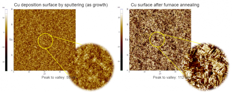
Scanning Conditions
- System : NX-Wafer
- Scan Mode: Non-contact
- Scan Rate : All 1Hz
- Scan Size : All 512μm×256μm
- Pixel Size : 512×512
- Cantilever : OMCL-AC160TS (k=26N/m, f=300kHz)