-
PhaseImaging Display GranadaUniv Grain SurfaceChange OpticalWaveguide SiliconeOxide Device nanomechanical CuFoil PUR SicMosfet HighAcpectRatio UTEM MoS2 UnivMaryland temperature_control DeflectionOptics Optoelectronic ForceDistanceSpectroscopy mechanical property Stiffness TappingMode Tungsten_disulfide single_layer graphene_hybrid Ferrite FM_KPFM Forevision InLiquid Polyethylene PMNPT Molybdenum_disulfide LateralForce FM_SKPM
Report image
If you found this image unacceptable, please let us know. We will review your report and take action if we determine this image is really unacceptable.
Photoresist pattern (post-development process)
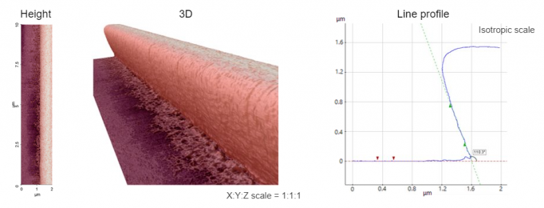
Scanning Conditions
- System : NX-3DM
- Scan Mode: Non-contact
- Scan Rate : 0.1 Hz
- Scan Size : 2μm×10μm
- Pixel Size : 512×2048
- Cantilever : EBD-R2-NCLR (k=45N/m, f=190kHz)