-
Phosphide pinpoint mode HOPG BaTiO3 Sidewall Lanthanum_aluminate Mechanical Current VerticalPFM LMF Filter SmalScan vertical_PFM LDPE MESA structure Tin sulfide PpLdpe Vac Zagreb alkanes AnodizedAluminumOxide ElectrostaticForceMicroscopy NiFe BismuthFerrite VinylAlcohol ThermalDetectors Mosfet CompactDisk STM Grain Spincast Pvdf solar_cell Floppy Fendb
Report image
If you found this image unacceptable, please let us know. We will review your report and take action if we determine this image is really unacceptable.
Chip
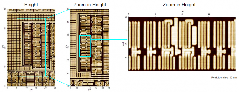
Scanning Conditions
- System : NX-Wafer
- Scan Mode: Non-contact
- Scan Rate : All 1Hz
- Scan Size : 25μm×40μm, 15μm×40μm, 8μm×4μm
- Pixel Size : 2048×256, 2048×256, 1024×256
- Cantilever : OMCL-AC160TS(k=26N/m, f=300kHz)