-
Ceramics MfmPhase Ptfe dichalcogenide Hafnia HafniumDioxide Nanopattern Ucl sputter LateralPFM Insulator Protein CeramicCapacitor multi_layer Polymer MLCC Grain CVD amplitude_modulation Workfunction Ito Co/Cr/Pt Optoelectonics fe_nd_b CNT SingleLayer Conduct Hexylthiophene NUSNNI DeflectionOptics Gold EFMAmplitude AM-KPFM Celebration SurfaceOxidation
Report image
If you found this image unacceptable, please let us know. We will review your report and take action if we determine this image is really unacceptable.
Patterned Sapphire Substrate (PSS)
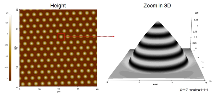
Scanning Conditions
- System: NX10
- Scan Mode: Non-contact
- Cantilever: AR5T-NCHR
- Scan Size: 40μm×40μm, 3μm×3μm
- Scan Rate: 0.3Hz, 1Hz
- Pixel: 256 × 256
- Scan Mode: Non-contact
- Cantilever: AR5T-NCHR
- Scan Size: 40μm×40μm, 3μm×3μm
- Scan Rate: 0.3Hz, 1Hz
- Pixel: 256 × 256