-
HACrystal Ucl Croatia ContactModeDot self_assembly Granada Neodymium Inorganic_Compound Epoxy Perovskite PvdfFilm Yeditepe_University Annealing Sperm Polydimethylsiloxane GaP medical mfm_amplitude Yeditepe Logo Leakage kelvin probe force microscopy HDD Chemical Vapor Deposition MetalCompound semifluorinated alkane SRAM flakes PinpointPFM PolycrystallineFerroelectricBCZT Metal HardDisk membrane HanyangUniv molecules
Report image
If you found this image unacceptable, please let us know. We will review your report and take action if we determine this image is really unacceptable.
BN thin film on Si
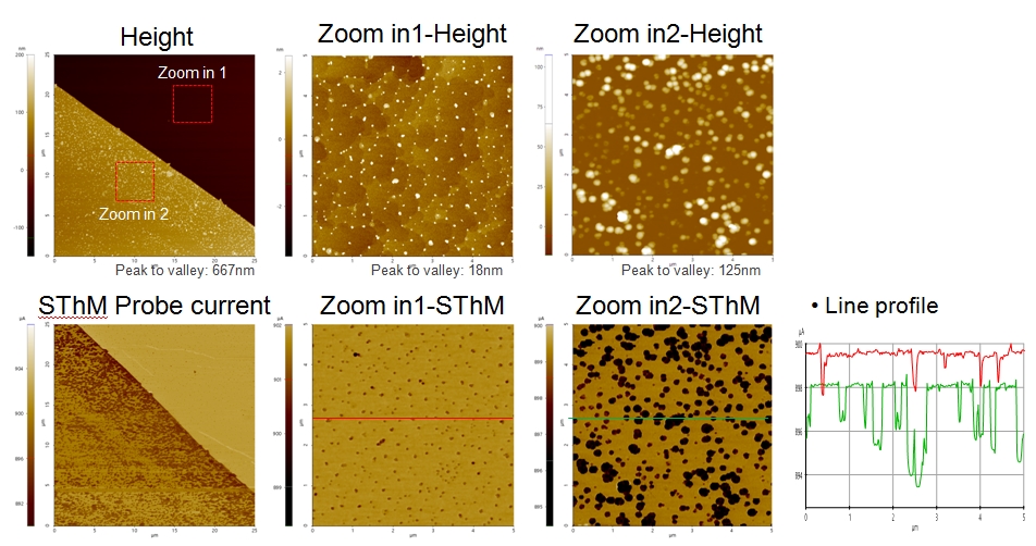
Scanning Conditions
- System: NX10
- Scan Mode:SThM
- Cantilever: Nanothermal probe
- Scan Size: 25μm×25μm, 5μm×5μm
- Scan Rate:0.3Hz, 0.5Hz
- Pixel: 256×256, 256×256
- Scan Mode:SThM
- Cantilever: Nanothermal probe
- Scan Size: 25μm×25μm, 5μm×5μm
- Scan Rate:0.3Hz, 0.5Hz
- Pixel: 256×256, 256×256