-
Ptfe MESA structure amplitude_modulation INSP Sapphire Electrical&Electronics MultiLayerCeramicCapacitor Galfenol Liquid PolyvinylAcetate plastic CalciumHydroxide organic_polymer Phthalocyanine AnodizedAluminumOxide Transparent Lift conductive Chemical_Vapor_Deposition ConductiveAFM rubber CNT Adhesive Litho Defect LiquidCell DeflectionOptics Force-distance Strontium P3HT electrospinning LiNbO3 pulsed_laser_deposition FrictionalForce TemperatureControl
Report image
If you found this image unacceptable, please let us know. We will review your report and take action if we determine this image is really unacceptable.
Atomic steps on GaP(Gallium Phosphide) layer on Si
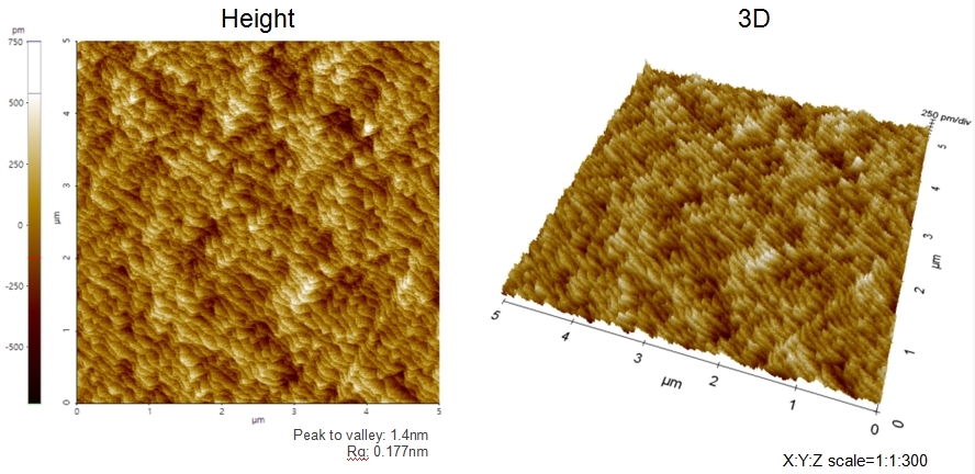
Scanning Conditions
- System: NX20
- Scan Mode: Non-contact
- Cantilever: PPP-NCHR (k=42N/m, f=300kHz)
- Scan Size: 5μm×5μm
- Scan Rate: 1Hz
- Pixel: 512×512